|
Thin-layer
silicon is considered to be <50-μm thick
and deposited on a foreign substrate. Potential advantages of thin-layer approaches include less Si
usage, lower deposition temperatures relative to melt growth, monolithic
module construction possibilities, and a tolerance for lower t
(the distance charge carriers have to travel is shorter). Disadvantages include incomplete light absorption (see Silicon
Light Absorption) and therefore the probable need for light-trapping, a
likelihood that grain sizes will be small, and difficulty in making rear
contacts if the substrate is an insulating material.
The
R&D challenge for successful thin-layer Si is to produce a 10- to 50-μm
silicon layer of sufficient electronic quality with a diffusion length
greater than the layer thickness and a grain size comparable to the
thickness. A fast deposition rate of >1μm/min
on a low-cost substrate such as glass is needed.
There is not yet any significant quantity of thin-layer
crystalline Si in commercial production for PV because only partial
successes have been achieved in meeting the challenge.
What has been accomplished follows:
-
Fast
epitaxy (1 μm/min)
of high-quality Si layers at intermediate temperatures (700°-900°C),
e.g., by liquid-phase epitaxy (LPE) but
on Si substrates
-
Low-T
(<600°C)
epitaxial growth of high-quality Si layers (e.g., by chemical vapor
deposition (CVD) but at
low growth rates (<0.05 μm/min)
and on Si substrates
-
Low-T
poly/microcrystalline 10% cells but at slow growth rates
-
Low-T
micro/amorphous direct-gap 13% cells but at slow growth rates
-
Fast
CVD at intermediate T on foreign substrates but
with sub-micron grain sizes
-
Fast
CVD of >1-μm
grain-size layers on foreign substrates but
at high T (~1200°C)
and with contamination
-
Smooth
Si at intermediate T by solid-state crystallization but
at slow rates, from slowly grown a-Si layers, and highly stressed.
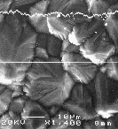
| A new
approach to iodine vapor transport growth (Wang and Ciszek, 2000)
shows considerable promise, and has achieved 5- to 20-μm-thick
Si layers with 5- to 10-μm
grain sizes at 1- to 10-μm/min growth rates directly on hi-T
glass at 850°-950°C.
The layers have 5 μs effective minority-carrier
lifetimes, which implies diffusion length >> layer thickness
and a low impurity content. A
scanning electron microscopy (SEM) photomicrograph of a layer is
shown here, along with an electron-beam induced current (EBIC) scan (upper
jagged line) that shows nearly uniform response on a scan line
(straight horizontal line) that crosses several grain
boundaries. This layer was grown at 3 μm/min
and is 30 μm
thick.
_______________________
T.H.
Wang and T.F. Ciszek, “Growth of Large-Grain Silicon Layers by
Atmospheric Iodine Vapor Transport,” J. of the Electrochem. Soc,
147 (5) (2000) pp. 1945-1949.
|
|