|
|

|
|
Silicon Info: Single-Crystal Ingot Growth
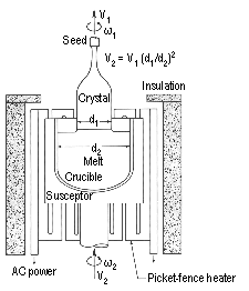
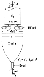
The single-crystal growth methods,
float-zoning (FZ) and Czochralski growth (CZ), are relatively well-known,
so only some aspects pertinent to PV applications will be addressed here. The table below compares the characteristics of the FZ and CZ methods. There are two principal technological advantages of the FZ method
for PV Si growth. The first
is that large t
values are obtained as a result of higher purity and better microdefect control,
resulting in 10% to 20% higher solar cell efficiencies.
The second is that faster growth rates and heat-up/cool-down times,
along with absences of a crucible and consumable hot-zone parts, provide a
substantial economic advantage. The
main technological disadvantage of the FZ method is the requirement for a
uniform, crack-free cylindrical feed rod.
A cost premium (100% or more) is associated with such poly rods.
At the present time, FZ Si is used for premium high-efficiency cell
applications and CZ Si is used for higher-volume, lower-cost applications.
Comparison of the CZ and FZ Growth Methods
Electrical power requirements for these two methods are on the order of 30kWh/kg for FZ growth and 60 kWh/kg for CZ growth in the IC industry. The more cost-conscious PV industry has been achieving 35-40 kWh/kg for CZ growth, and some recent experiments indicate that levels on the order of 18 kWh/kg may be achieved for 150-mm-dia. crystals by using improved insulation materials and lower argon-gas flow rates (Mihalik et al., 1999). Not only were energy requirements reduced, but also argon consumption was reduced from 3 m3/kg of Si to 1 m3/kg of Si. Also, oxygen content in the crystals was reduced by 20%, the crystal growth rate was increased from 1.28 kg/hr to 1.56 kg/hr, and relative solar cell efficiency increased by 5%. In CZ Si PV technology, approximately 30% of the costs are in the crystal ingot, with 20% in wafering, 20% in cell fabrication, and 30% in module fabrication. High-speed wire saws that can wafer one or more entire ingots in one operation have greatly improved the throughput of the wafering process. A wire saw can produce about 500 wafers/hour compared to about 25 wafers/hour for older inside-diameter (ID) saw technology. Furthermore, it creates shallower surface damage (10 μm) than the ID saws (30 mm), and allows thinner wafers to be cut, thus increasing the number of wafers per ingot. Currently, about 20 wafers are obtained from 1 cm of ingot. Efforts are under way to obtain 35 wafers/cm. Problems with increased breakage are seen with the thinner wafers - especially in the sawing process. At 20 wafers/cm and a wafer thickness > 300 μm, breakage is on the order of 15%. This can rise to on the order of 40% when the wafer thickness is decreased to 200 μm. It is clear that wafer handling will be an important issue as wafers become thinner. One clever way of dealing with the low fracture strength of thin (100) wafers from single-crystal CZ ingots is to deliberately introduce a controlled multicrystalline structure into the growing ingot. In particular, the tricrystalline structure described by Martinelli and Kibizov (1993) provides three grains propagating along the length of the ingot. Each has a <110> longitudinal direction. Two of the grain boundaries are first-order {111} twin planes, and the third is a second-order {221} twin plane. The three angles between boundaries are thus 125.27o, 125.27o, and 109.47o. The twins block any {111} planes from crossing entirely across the ingot, and improve the resistance to cleavage or propagation of defects that takes place on {111} planes. Wafers from these tricrystals are observed to possess about 440 MPa fracture strength compared to about 270 MPa for (100) single-crystal wafers and 290 MPa for multicrystalline wafers (Endros et al., 1997). The measurements were made on wafers after etching in KOH at 100oC to 310-mm thicknesses. Breakage during wire sawing of tricrystal ingots at <200 mm thickness is half of that for <100> ingots. The tricrystal ingots have been shown to maintain their structure for reasonably long lengths (150-400 mm at the present state of technology) with minimal degradation of minority carrier recombination properties (Wawer et al., 1997).
Continuous, dislocation-free, single-crystal
Czochralski growth now dominates PV technology with over 80% market share, as it
provides the high minority-charge-carrier lifetimes needed to take advantage of
high-efficiency cell and module processes.
|
|
♦♦♦♦♦ ted_ciszek @ siliconsultant.com (remove spaces) ♦♦♦♦♦
|