A multicrystalline structure with grains on
the order of mm to cm in width and approximately columnar along the
solidification direction is characteristic of directional solidification (DS)
or casting in crucibles, and also of electromagnetic semicontinuous
casting. Casting of
multigrain silicon was reported more than 80 years ago (Allen, 1913). In 1960, large multicrystalline-silicon domes and plates 330
mm in diameter by 50 mm thick were formed via ambit casting.
Early applications were for infrared optics and other
non-semiconductor uses. A
summary of early silicon casting approaches was compiled by Runyan (1965).
Si casting into graphite molds as an alternative to CZ growth for
PV applications was reported by Fischer and Pschunder (1976).
|
|
|
Directional
Solidification/Casting |
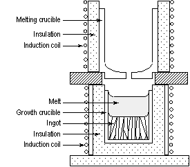
DS
can be carried out in a separate crucible after (or as) silicon is poured
into it from a melting crucible, as indicated in the figure above.
This process is usually referred to as silicon casting.
Or, the silicon can be melted and directionally solidified in the
same crucible (e.g., the bottom crucible).
This technique is referred to as directional solidification.
It is simpler than casting, because no melt pouring is involved,
but there are longer reaction times at high temperature between the melt
and the crucible, as well as longer turnaround times.
Because melting and solidification are decoupled in casting, higher
throughputs are possible. But
the process and equipment are more complex.
DS
of silicon in the same quartz (fused silica) crucible used to melt it
would seem to be a logical approach for large-grained ingot production,
but sticking and thermal expansion mismatch between the solidified Si and
the crucible lead to significant cracking problems.
This was alleviated to some extent by deliberately weakening the
inner wall of the quartz crucible (Khattak and Schmid, 1978).
High-density graphite crucibles were introduced for DS as a way of
avoiding the cracking (Ciszek, 1979).
Most crucible-based commercial methods of growing
multicrystalline Si ingots for PV consumption use either the casting
method or DS in the melting crucible.
The crucibles are either graphite or quartz (often coated with Si3N4
or other compounds to discourage sticking or enable reuse). The actual growth process is DS in either method.
Multicrystalline
ingots as large as 690 mm x 690 mm in cross section and weighing as much
as 240 kg are grown in total cycle times of 56 hours.
The resultant throughput is 4.3 kg/h.
Thus, the larger area, compared to CZ crystals, more than offsets
the somewhat lower linear growth rates leading to higher throughputs for
DS by a factor of ~3. Either
induction heating or resistance heating can be used.
The energy consumption for DS is in the range of 8-15 kWh/kg.
Unlike CZ growth, the solid/liquid interface is submerged in DS,
and precipitates or slag at the melt surface do not disrupt growth.
DS is a simpler process requiring less skill, manpower, and
equipment sophistication than CZ growth, which can make it a lower cost process.
However, there are also drawbacks.
There are numerous crystal defects (grain boundaries and
dislocations) due to the multicrystalline structure.
Impurity contents can be higher depending on the crucibles used,
and portions of the bottom, sides, and top surface of the ingot are
discarded. So, the lower cost of DS is at the expense of solar cell
efficiency. DS solar cells
are about 85% as efficient as CZ cells.
The best efficiency of small cells, with sophisticated processing,
is 18.6%. Typical large
production cell efficiencies are 13%-14%, with good consistency.
|
|
|
Electromagnetic Casting |
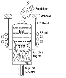
Electromagnetic
casting (EMC), shown here, has some similarities to
the casting and DS methods just described, but also has several unique
features that change the ingot properties and warrant a separate
discussion. The method
was first applied to semicontinuous silicon ingot casting by Ciszek (1985,
1986). EMC is based on
induction-heated cold-crucible melt confinement, except that unlike the
conventional cold crucible, there is no crucible bottom.
A parallel, vertical array of close-spaced, but not touching,
water-cooled, conducting fingers is attached at one end to a water-cooling
manifold. The other end of
each finger is closed. An
internal distribution system carries cooling water to the tip and back
again. The shape of the
region enclosed by the close-spaced fingers determines the cross section
of the cast ingot, and a wide variety of shapes are possible (circular,
hexagonal, square, rectangular, etc.).
Silicon is melted on a vertically moveable platform (typically
graphite) located within the finger array.
The melting is accomplished by induction heating after suitable
preheating. The induction
coil, placed outside the finger array, induces a current to flow on the
periphery of each finger, around the finger's vertical axis.
Like a high-frequency transformer, each finger in turn induces a
current to flow in the periphery of the silicon charge, about its vertical
axis. The silicon is heated
by its resistance to the current flow.
There is Biot and Savart-law repulsion between the current flowing
in the periphery of the silicon melt and the currents flowing in the
fingers, because they are induced to flow in opposite directions at any
particular instant in the RF cycle. Thus, the melt is repulsed from the water-cooled fingers.
The open-bottom arrangement allows the platform to be withdrawn
downward, solidifying the molten silicon, while new melt is formed by
introducing feed material from the top.
In this way, a semicontinuous casting process can be carried out.
A
variety of feed silicon geometries can be used (melts, rods, pellets,
scrap, etc.).
Because the interface is submerged, feed perturbances or slag at
the melt surface do not affect the solidification front.
Ingot lengths of 3 m have been demonstrated.
The cross section of the ingots has evolved over years of
development and is currently about 350 mm x 350 mm. The cold fingers allow
steep thermal gradients and fast growth speeds (~1.5-2.0 mm/min), even in
ingots with large cross sections.
But they also cause a steeply curved interface that is concave
toward the melt.
Thus, grains are neither as columnar nor as large as in
conventional DS.
The average grain size is on the order of 1.5 mm in large ingots.
This decreases
τ,
but the relatively high purity and freedom from oxygen and carbon
impurities (O < 6x10¹⁵; C < 8x10¹⁶) largely
offset the grain-size effect, so that solar cell efficiencies of about
14%-15% are obtained on 15 cm x 15 cm cells.
The throughput of EMC is the highest of any ingot growth technique
- up to approximately 30 kg/h. The
power consumption is about 12 kWh/kg.
As PV technology progressed, cell efficiencies
increased and higher minority charge carrier lifetimes were necessary to
achieve them. The trend in crystal growth methods went from large
directionally solidified multicrystalline ingots to dislocation-free single
crystals grown by the Czochralski method. CZ growth dominates the
technology now with over 80% market share.
__________________________
Allen, T.B. (1913) U.S. Patent 1,073,560.
Ciszek, T.F. (1979) J. Crystal Growth 46,
527.
Ciszek, T.F. (1985) J. Electrochemical Soc. 132,
963.
Ciszek, T.F. (1986) U.S. Patent 4,572,812.
Fischer, H., and Pschunder, W. (1976) IEEE
12th Photovoltaic Specialists Conf. Record, IEEE, New York,
86.
Khattak, C.P., and Schmid, F. (1978) IEEE
13th Photovoltaic Specialists Conf. Record, IEEE, New York,
137.
Runyan, W.R. (1965) "Silicon Semiconductor Technology" McGraw-Hill
Book Company, New York. |