Past
Work: Electromagnetic Casting
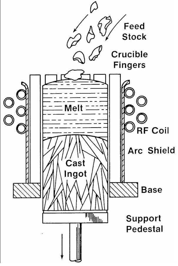
We discovered and patented the semicontinuous electromagnetic cold-crucible casting
technique for silicon in the mid-1980s1,2 . This method has a higher throughput than any other Si ingot technology,
because of the easy heat transfer to a cold environment. A trade-off is that grain
size is small because of the rapid cooling. However, the purity level is very high
because this is essentially a "containerless" method. All things
considered, the method makes >13%-efficient production cell efficiencies at a high
throughput. While it has not caught on in the US, it has been more vigorously
developed in Europe and Japan, where ingots weighing over 40 kg with cross sections
greater than 35 x 35 cm are produced.
|
___________________________
1. Theodore F. Ciszek, "Method and
Apparatus for Casting Conductive and Semiconductive Materials," U.S. Patent 4,572,812,
1986.
2. T.F.
Ciszek, "Some Applications of Cold Crucible Technology for Silicon
Photovoltaic Material Preparation," J. Electrochemical Soc. 132
(1985) 963.
|