|
| |
Technical Background
 |
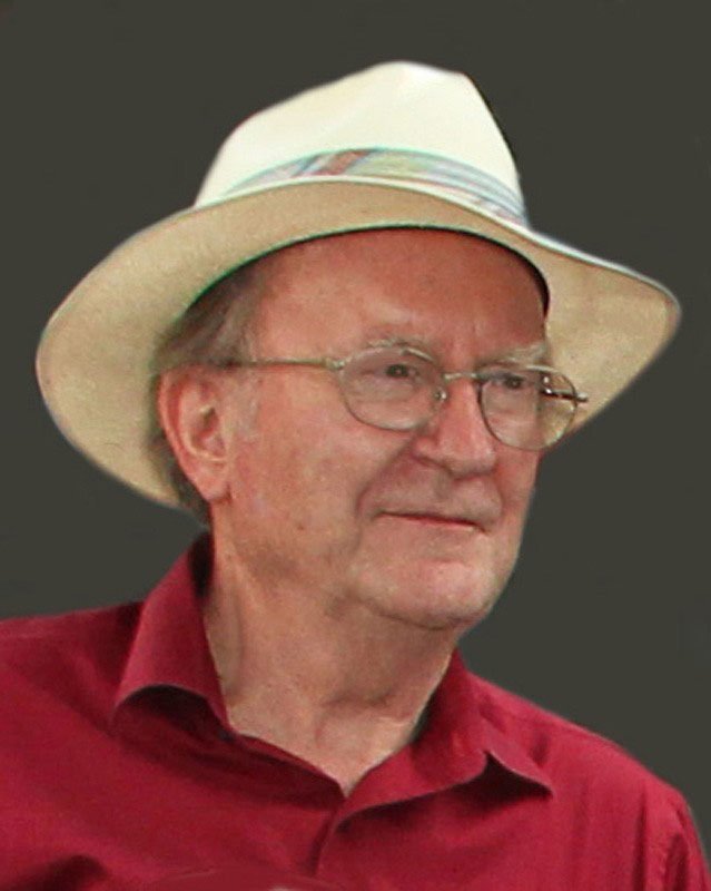
Ted
Ciszek has worked 52 years in the areas of silicon crystal growth,
characterization, defect and impurity studies, and materials research - most
recently as a private consultant after retiring as Principal Scientist and group leader for the Silicon Materials Research
Task at NREL, the National Renewable Energy
Laboratory, in Golden, Colorado. He joined NREL (then SERI) in 1978, after spending 6 years each
with Dow Corning (at what is now HSC, the Hemlock Semiconductor
Corporation) in Hemlock, Michigan and IBM in East Fishkill, NY. At Dow
Corning, he researched dislocation-free float-zone (FZ) Si growth and
electron-beam pedestal growth, and grew the first EFG Si ribbons. He
holds over 180 technical papers and 25 patents on crystal growth, electronic and superconductor
materials, and characterization. He is now consulting on silicon
materials. |
|
|
| Education |
B.S.
Physics (1964) Case Institute of Technology; M.S. Physics (1966) Iowa State
University. |
|
|
| Professional
Activities |
AACG
(held posts as VP, Executive Committee member, meeting chairman); APS; ECS
(Electronics Div. editor, J. Electrochem. Cos. to 1989). |
|
|
| Honors |
3 NASA
Certificates of Recognition for PV materials work; IBM Invention Achievement
Award; SERI 1981 Outstanding Achievement Award; 1990 DOE Peer Review Award;
NREL 2002 Hubbard Award for "exceptional leadership and sustained,
world-class research contributions in the successful development of silicon
crystal growth"; Member Tau Beta Pi and Sigma Xi; Technical Advisory Committee
member for several major EPRI/DOE-funded research projects. |
Major
technical contributions:
| 1967-72
Dow Corning Corporation: Developed Perfx process for dislocation-free
float-zoned silicon crystals. Introduced
[115] growth orientation for low surface-state charge density
applications. Invented silicon pedestal
growth process with electron-beam heating.
Grew the first reported EFG silicon ribbons using a graphite capillary die.
|
| 1972-78
IBM:
Developed the EFG/CAST technique for Si ribbon growth.
Invented shaped crystal growth from wettable projections.
Achieved in-situ melting and crack-free directional solidification of
silicon in graphite crucibles. Grew
the first reported EFG silicon tubes. Invented contiguous capillary coating technique for silicon sheet
growth (early version of later S-web growth process).
Established a float-zone Si crystal growth laboratory.
|
| 1978-2003
SERI/NREL: Invented edge-supported pulling method for Si sheet growth
(string ribbon). Established laboratory
facilities for silicon, compound semiconductor, and superconductor crystal
growth, sheet growth, and
characterization (including x-ray topography and carrier lifetime). Conducted
silicon crystal growth for high-efficiency photovoltaics and achieved
minority charge-carrier lifetimes >20 milliseconds.
Conducted numerous Si defect and impurity studies using FZ. Grew thin-layer silicon LPE from metal solutions.
Invented semicontinuous electromagnetic casting EMC technique for
silicon. Devised new methods for CuInSe2 crystal growth and CuAgInGaSe2 solid solution crystal growth. Grew
single crystals, sheets, rods, and wires of the YBCO and BiSCCO high Tc
superconductors. Researched several new PV
Si feedstock methods. Served as Principal Investigator for NREL's
small, in-house crystalline silicon R&D program.
|
|