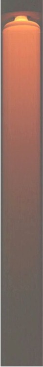
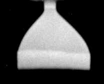
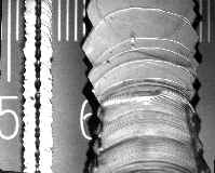
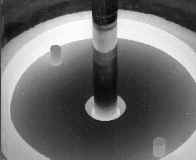
To explore crystal growth of thin
Si filaments for potential use in applications such as PV multi-concentrator arrays, IR light guides,
and delay lines, we used three methods:
-High-purity, single-crystal pedestal float-zoning (top)
-Rapid dendrite growth from supercooled melts (middle)
-Solidifying tubular filaments from capillary dies (bottom).
Charge-carrier
lifetimes
of 660 μs, 53 μs, and 42 μs were seen,
respectively. This work was a feasibility
demonstration. Some X-ray topographic and lifetime characterization was carried out,
but additional effort would be needed to fully characterize the materials and demonstrate
devices. For more details, see the references below.
______________
T.F.
Ciszek and T.H. Wang, "Growth and Properties of Silicon Filaments for Photovoltaic
Applications," in: 26th IEEE Photovoltaic Specialist Conf.
Record, Anaheim, CA, Sept.
29-Oct. 3, 1997 (IEEE, New Jersey, 1997) pp. 103-106.
T.F. Ciszek and T.H. Wang,
"Float-zone Pedestal Growth of Thin Silicon Filaments," in: High Purity Silicon
V, Eds. C.L. Claeys, P. Rai-Choudhury, M. Watanabe, P. Stallhofer, and H.J. Dawson (The
Electrochemical Soc., Proceedings Volume 98-13, New Jersey, 1998) pp. 85-89.
|
 |