The challenge
for Si thin-layers on foreign substrates in PV applications is to produce an active Si layer of sufficient electronic quality,
with a thickness on the order of 10 μm,
and at a fast deposition rate of about 1 μm/min
on a low-cost substrate such as glass. The principal electronic
quality requirement is a long minority-carrier diffusion length comparable to the layer thickness,
which demands that the grain size be similar. Unfortunately, efforts
around the world have thus far only resulted in partial solutions (e.g., fast epitaxy of high-quality layers
on Si substrates, fast deposition of submicron-grain-size layers on high-temperature
glass, or slow solid-state crystallization from slowly deposited a-Si layers yielding
stressed films).
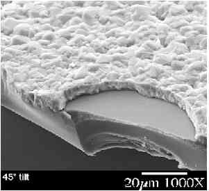
We had partial
success with a gas-phase growth technique that produces continuous Si layers of
5-20-μm thickness with
5-10-μm grain size on high-temperature glass at a
growth rate of 1-10 μm/min. So far, the layer quality is not sufficient, and more work is needed to improve
its properties and PV performance.
 |
SEM Photo of thin Si layer
on glass |

|
SEM Photo of thin Si
layer on glass - Top View |
|